Counting Memory Read and Write Operation in 8085
Auto Cycle in 8085 Microprocessor:
The seven Machine Cycle in 8085 Microprocessor are :
- Opcode Fetch Cycle
- Retentiveness Read
- Retentiveness Write
- I/O Read
- I/O Write
- Interrupt Acknowledge
- Coach Idle
1. Opcode Fetch Bike:
The showtime Car Cycle of 8085 Microprocessor of every instruction is opcode fetch cycle in which the 8085 finds the nature of the pedagogy to exist executed. In this Machine Wheel in 8085, processor places the contents of the Program Counter on the address lines, and through the read procedure, reads the opcode of the didactics. Fig. ane.15 (a) shows flow of data (opcode) from retentiveness to the microprocessor and Fig. 1.15 (b) shows the timing diagram for Opcode Fetch Automobile Cycle 8085. The length of this cycle is not fixed. It varies from 4T states to 6T states as per the instruction. The post-obit section describes the opcode fetch cycle in step past pace manner.
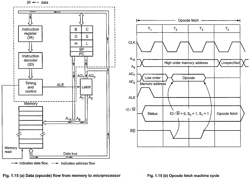
Step ane : (State Ti): In T1 state, the 8085 places the contents of program counter on the accost bus. The high-order byte of the PC is placed on the A8 – Afifteen lines. The depression-order byte of the PC is placed on the Advertizing0 – AD7 lines which stays on simply during T1. Thus microprocessor activates ALE (Address Latch Enable) which is used to latch the depression-social club byte of the address in external latch before it disappears.
In T1, 8085 too sends status signals IO/M, Si, and S0. IO/K specifies whether it is a retentivity or I/O operation, S1 status specifies whether it is read/write operation; Sane and S0 together indicates read, write, opcode fetch, machine cycle performance, or whether it is in HALT land. In opcode fetch machine cycle status signals are : IO/K = 0, Southwardi = 1, Southward0 = 1.
Step ii : (Country T2) In Ttwo, low-lodge accost disappears from the AD0 – AD7 lines. (Withal A0 – Avii remain available as they were latched during T1). In Tii, 8085 sends RD signal low to enable the addressed memory location. The memory device so places the contents of addressed retention location on the data bus (AD0 – Ad7).
Stride 3 : (Country T3) During T3, 8085 loads the data from the data autobus in its Instruction Register and raises RD to high which disables the memory device.
Step four : (State Tfour) In Tfour, microprocessor decodes the opcode, and on the ground of the teaching received, it decides whether to enter country Tfive or to enter state Tane of the next Machine Wheel of 8085 Microprocessor. 1 byte instructions those operate on 8 bit data (8 chip operand) are executed in T4.
For instance : MOV A, B, ANA D, Add B, INR L, DCR C, RAL and many more.
Notation : For 1 byte instructions which operate on eight chip data, information is always bachelor in the internal memory of 8085 i.eastward. registers.
Step 5 : (Land Tfive and Tvi) State T5 and T6, when entered, are used for internal microprocessor operations required past the instruction. During T5 and T6 , 8085 performs stack write, internal sixteen chip; and conditional render operations depending upon the type of instruction. Ane byte instructions those operate on sixteen bit data (16 bit operand) are executed in T5 and T6. For case DCX H, PCHL, SPHL, INX H, etc.
2.Retentiveness Read Bicycle:
The 8085 executes the memory read wheel to read the contents of R/W memory or ROM. The length of this machine cycle is 3-T states (T1 – Tiii). In this Machine Cycle in 8085, processor places the address on the accost lines from the stack pointer, general purpose annals pair or program counter, and through the read procedure, reads the information from the addressed memory location. Fig. 1.16 (a) shows flow of data from memory to the microprocessor and Fig. 1.16 (b) shows the timing diagram for retentivity read machine cycle. Retentiveness read automobile cycle is similar to the opcode fetch auto cycle. All the same, they use only states T1 to Tiii, and the condition point values (IO/Yard = 0, Sone = 1, S0 = 0) appropriate for retention read machine cycle are issued in T1.
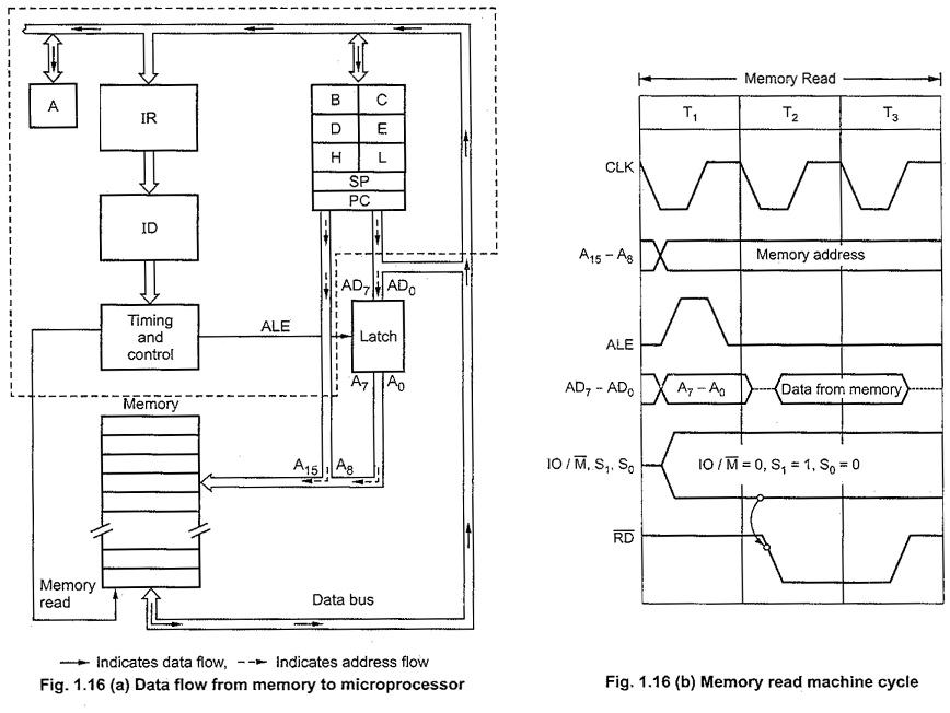
The following section describes the memory read machine cycle in step by pace manner.
Pace i : (State Tone) In Tane land, microprocessor places the address on the accost lines from stack arrow, full general purpose register pair or program counter and activates ALE signal in lodge to latch low-order byte of address.
During Tone, 8085 sends status signals : IO/M = 0, Sone = ane, and South0 = 0 for memory read machine cycle.
Step 2 : (State T2) In Tii, 8085 sends RD signal low to enable the addressed retention location. The memory device and so places the contents of addressed retentiveness location on the data jitney (AD0 -ADseven).
Step 3 : (Land T3) During T3, 8085 loads the data from the information jitney into specified register (F, A, B, C, D, E, H, and 50) and raises RD to high which disables the memory device.
3.Retentiveness Write Cycle:
The 8085 executes the memory write wheel to store the data into data memory or stack memory. The length of this machine bike is 3T states. (T1 – T3). In this Car Wheel of 8085 Microprocessor, processor places the address on the accost lines from the stack pointer or general purpose register pair and through the write process, stores the data into the addressed retentivity location. Fig. one.17 shows the timing diagram for retentiveness write machine cycle. The retentiveness write timing diagram is similar to the memory read timing diagram, except that instead of RD, WR indicate goes low during Tii and T3. The status signals for memory write cycle are : IO/One thousand = 0, Due south1 = 0, S0 = 1. The following section describes the memory write automobile bicycle in step by step way.
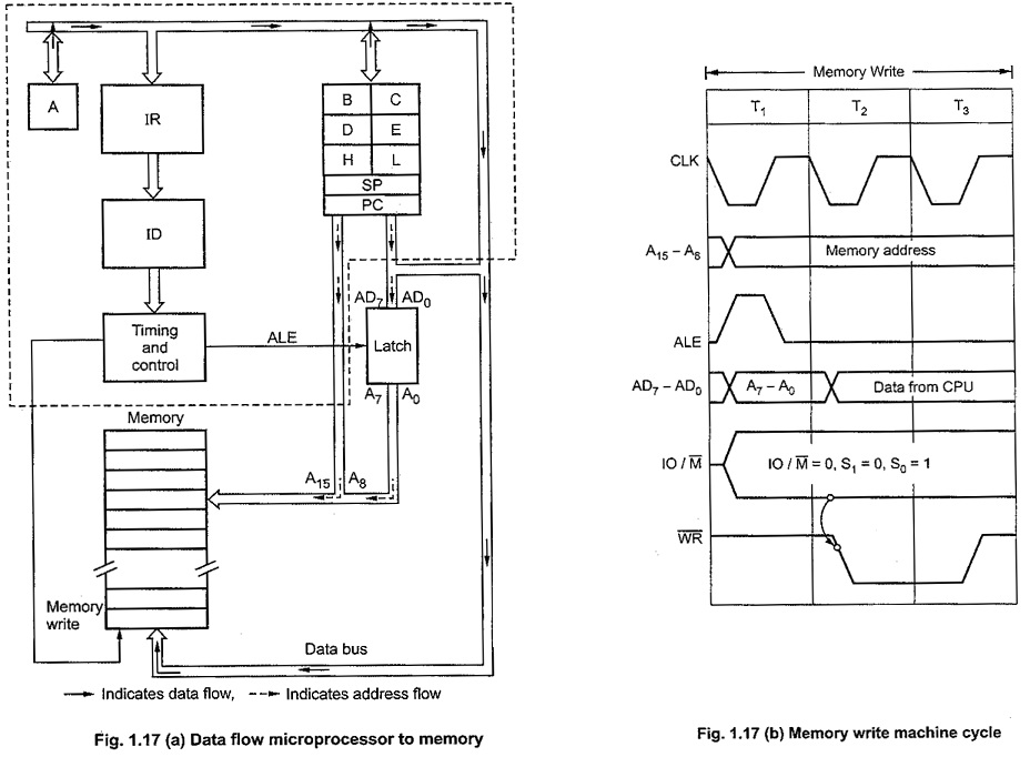
Footstep 1 : (Land Ti) In T1 state, the 8085 places the address on the address lines from stack pointer or general purpose register pair and activates ALE signal in social club to latch low-order byte of address. During T1, 8085 sends condition signals :
IO/1000 = 0, Southward1= 0 and S0 = 1 for retentivity write machine cycle.
Footstep 2 : (State T2) In T2, 8085 places data on the data bus and sends WR signal low for writing into the addressed memory location.
Step 3 : (State T3) During T3, WR signal goes high, which disables the memory device and terminates the write operation.
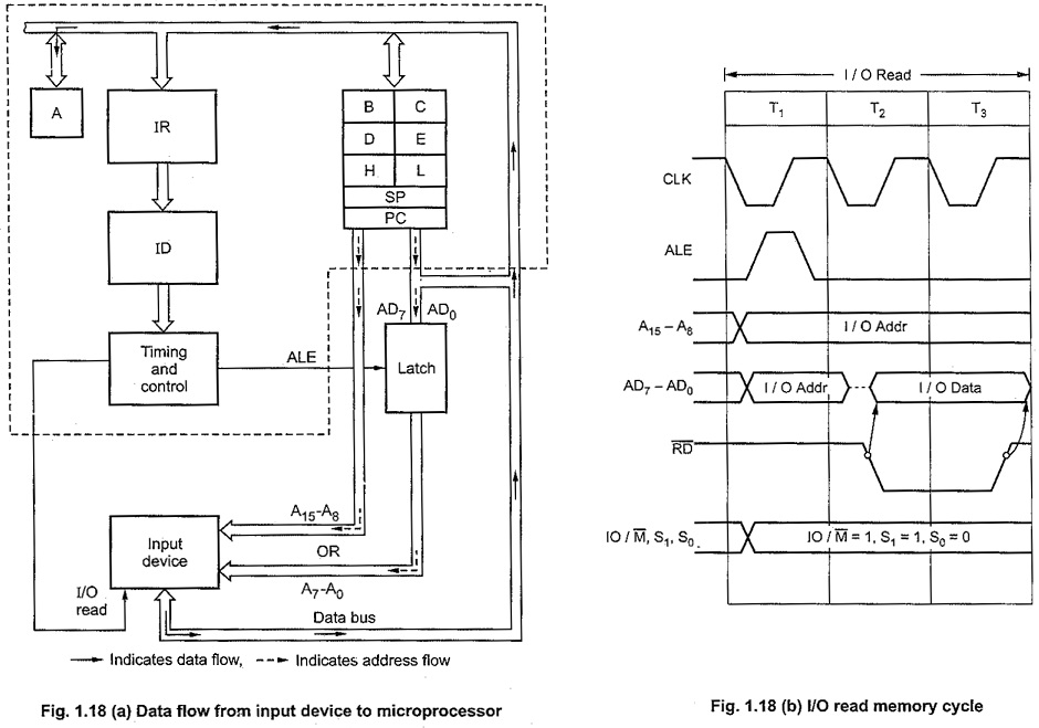
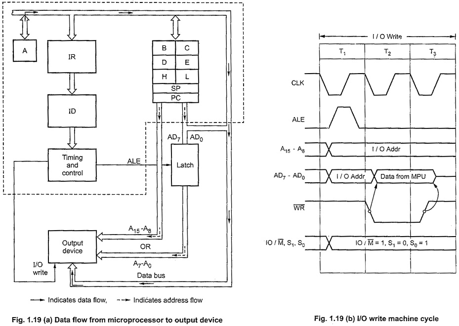
4, 5. I/O Read and I/O Write cycles:
The I/O read and I/O write automobile cycles are similar to the memory read and memory write car cycles, respectively, except that the 10/One thousand signal is loftier for I/O read and I/O write machine cycles. High IO/M bespeak indicates that it is an I/O operation. Fig. 1.eighteen (b) and Fig. 1.19 (b) show the timing diagrams for I/O read and I/O write cycles, respectively.
6. Interrupt Acknowledge Cycle:
In response to INTR signal, 8085 executes interrupt acknowledge machine bike to read an educational activity from the external device. Theoretically, the external device can place any instruction on the data motorcoach in response to INTA. However, only RST and Call, relieve the PC contents (return address) before transferring control to the interrupt service routine. The side by side sections explain Interrupt Acknowledge Wheel of 8085 for RST and Phone call instructions.
Interrupt Admit Cycle for RST didactics:
Fig. ane.twenty shows the timing diagram of the interrupt acknowledge car cycle and execution of RST instruction. The interrupt acknowledge cycle is similar to the opcode fetch cycle, with ii exceptions.
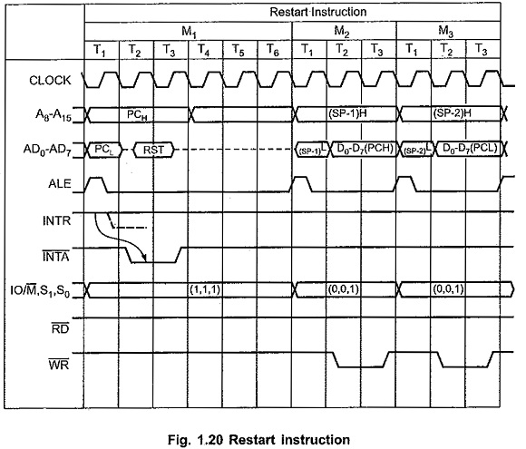
- The INTA signal is activated instead of the RD indicate.
- The condition lines (IO/M, S0 and S1) are 111 instead of 011:
During interrupt acknowledge automobile wheel (Mone), the RST is decoded, which initiates 1 byte CALL instruction to the specific vector location. The machine cycles Mii and M3 are memory write cycles that store the contents of the program counter on the stack, and then a new instruction wheel begins.
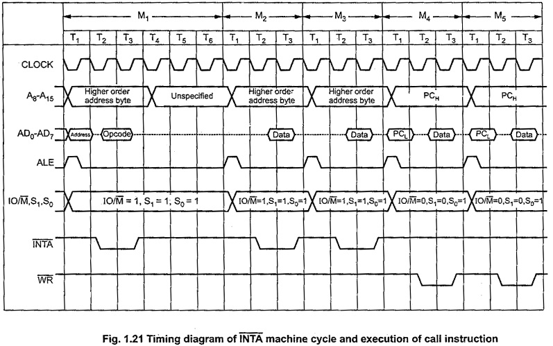
Interrupt Acknowledge Cycle for Phone call pedagogy:
Fig. 1.21 shows the timing diagram of the Interrupt Admit Bike of 8085 and execution of a CALL instruction. For Telephone call instruction, information technology is necessary to fetch the two bytes of the CALL address through 2 additional interrupt acknowledge machine cycles (M2 and Chiliad3 in the ane.21). The machine cycles Grand4 and Chiliad5 are memory write cycles that store the contents of the program counter on the stack, and so a new instruction cycle begins.
7. Omnibus Idle Wheel:
There are few situations where the automobile cycles are neither Read nor Write. These situations are:
one.For execution of DAD didactics (this instruction adds the contents of a specified register pair to the contents of HL annals pair) ten T states are required. This means that later on execution of opcode fetch machine cycle, DAD education requires 6 actress T-states to add together sixteen fleck contents of a specified register pair to the contents of HL register pair. These actress T-states which are divided into two machine cycles do not involve any retentivity or I/O operation. These Machine Cycle in 8085 are chosen BUS IDLE machine cycles. Fig. ane.22 shows Coach Idle Machine Wheel of 8085 Microprocessor for DAD instruction.
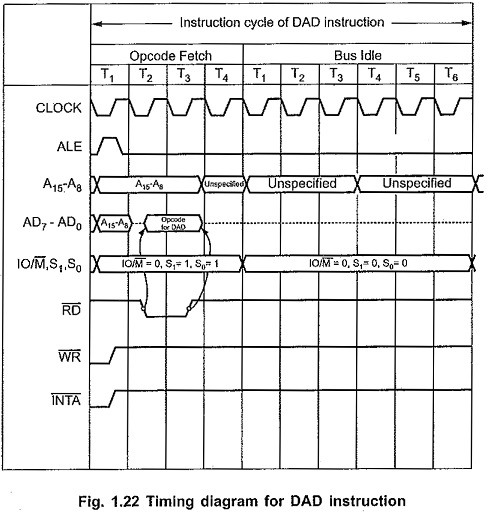
In the case of DAD, these Double-decker Idle cycles are similar to memory read cycles, except RD and ALE signals are not activated.
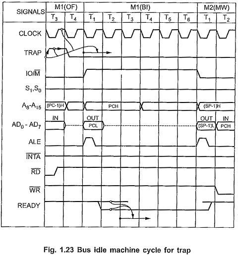
ii.During internal opcode generations, for TRAP and RST interrupts, 8085 executes Double-decker Idle Machine Cycles. Fig. 1.23 shows the Double-decker Idle Machine Cycle of 8085 Microprocessor for TRAP. In response to TRAP interrupt, 8085 enters into a Jitney Idle Car Bike during which it invokes restart instruction, stores the contents of PC onto the stack and places 0024H (Vector address of TRAP) onto_ the program counter.
The number of motorcar cycles required to fetch complete education depends on the didactics type :
- 1 byte ii. Two byte or iii. Three byte
One byte instruction doesn't require any additional machine bicycle. Two byte instruction requires one additional retentiveness read machine cycle, whereas three byte pedagogy requires ii additional memory read machine cycles.
The number of Machine Cycle in 8085 required to execute the pedagogy depends on the item instruction. The full number of machine cycles required varies from 1 to five. It is possible that retentiveness read and retentiveness write machine cycles occur more than once in a single instruction cycle. The post-obit examples illustrate the timing diagrams and machine cycles used for few 8085 instructions.
Concept of Wait States in 8085:
In some applications, speed of memory organisation and I/O system are not compatible with the microprocessor'due south timings. This means that they have longer time to read/write data. in such situations, the microprocessor has to confirm whether a peripheral is prepare to transfer information or not. If READY pin is loftier, the peripheral is prepare otherwise 8085 enters wait country.
Fig. 1.24 shows the timing diagram for retentiveness read machine cycle with and without await land.
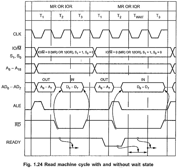
Concept of Wait States in 8085 continue to be inserted every bit long as READY is low. After the wait state, 8085 continues with T3 of the machine bicycle. During a expect state the contents of the address omnibus, the information coach, and the control omnibus are all held constant.
The expect state then gives an addressed retention or I/O port an actress clock bicycle fourth dimension to output valid information on the data bus. This feature allows to use cheaper memory or I/O devices that take longer access times.
Source: https://www.eeeguide.com/machine-cycle-in-8085-microprocessor/
0 Response to "Counting Memory Read and Write Operation in 8085"
Post a Comment